Beginning to troubleshoot digitizing video effects switchers to component level

Disclaimer: This article is not intended to take the place of any information otherwise supplied or sold by the manufacturer of the example equipment. The item chosen as the example equipment was selected because it was the opinion of the writer that it embodies excellent design practice and robust operational characteristics. All of the information contained herein is easily learned, without the aid of this article, by anyone competent enough in their own skills to read the schematics in the service manual which is available from the manufacturer.
In all cases, no service of such a complex product should ever be undertaken without the proper manuals, knowledge, and tools. Damage due to improper service attempts could easily amount to several thousand $US. In most cases, such an expensive and intricate product would be sent to a factory repair depot rather than be serviced by an independent party.
Furthermore, it is far beyond the scope of this article to discuss the exact modus operandi of all of the possible functions available on this switcher, but instead the goal is to introduce the technician to the concepts of signal and data flow within the unit so that a trouble may be efficiently located. If you are technogeek enough to bite this one off and chew on it, please read on and enjoy your trip into the outskirts of DSP-land as we open the kimonos on the Sony DFS500 and take a peek inside!...
Overview: The DFS500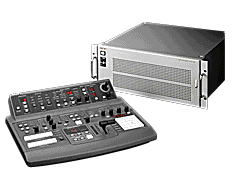
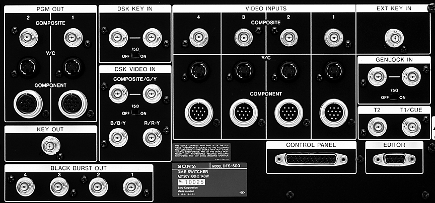
Rear Panel
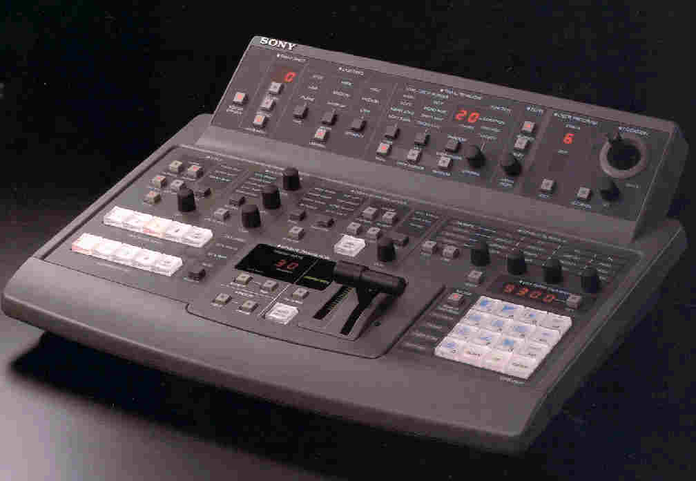
Keyboard
Scope:
For the sake of discussion, We will focus on the Sony DFS-500 switcher. This instrument has four inputs which can each be set for composite, Y/C, or component input signals. The 500 also has numerous special functions such as Chroma Key, DownStream Keying, and control interfaces for editors such as the BVE600 and others.
The SY board, power supply, and Keyboard will not be discussed as they are fairly easily diagnosed with only a general knowledge of switchmode regulator and microcontroller circuitry. The SY board and keyboard are provided with special diagnostics which are found in the service manual and the power supply may be tested by simply measuring the voltages.
When IC location numbers are mentioned, it is for reference later when using the schematics in the manual. At this time the discussion will be directed primarily to the block diagram level.
The switcher has two analog input busses, the A and B busses. To avoid confusion when referring to A, B, FG (FRGD, FOREGROUND), AND BG (BKRG, BACKGROUND) busses, it is important to remember that the A and B busses refer to those circuits carrying the analog input signals before the frame synchronizer, and that the FG and BG busses refer to those circuits carrying digitized A or B video for use as foreground or background video data throughout the DSP path (after the frame synchronizer).
Once the internal operations of the DFS-500 have been introduced, the engineer will find that troubleshooting the unit to component level is not only possible but fairly expedient.
You will need:
Extender card EX-326, part# J-6186-940-A
Waveform monitor with line select
Digital oscilloscope with line select
Service Manual
Signal generator
Video monitor
25 pin cable, part# 1-565-065-11
Note that when installed, the EX-326 card bypasses some of the "CP-Nxx" style solder-in fuses found on the various cards. Also, using a common 25 pin "computer cable" to connect the keyboard to the processor is incorrect and may result in damage to circuitry or blown fuses. Always use the 25 pin Sony cable.
DFS-500 Internals:
The DFS-500 switcher device processes the input analog video as component digital signals internally, regardless of whether the input signal is composite, Y/C, or component. The input video, if not already component, is converted to component before digitizing.
AD-76 Board
Input Signal Format; User Selection:
The input block of the unit is the AD-76 board. Each of the four input channels is configured for either Composite, Y/C, or Component with a slide switch on the front of the board. This is considered a setup procedure and is not generally used during an edit session as the switched are inside the front cover. The switches may, however, be set during operation and their effect is almost immediate.
Input Signal Format; Internal Logic:
Each input connector feeds its own IC input switch for each individual part of the signal present at that connector. This is to say that a composite input has a single pole switch, a Y/C input has a double pole switch, and a component input has a 3-pole switch.
Format/Bus selection block overview:
This analog switch block is therefore comprised of four single pole switches, four double pole switches, and four 3-pole switches per bus. Two busses, "A" and "B". are used. This block of switches is effected by IC101-112 and IC201-212. Control logic for the switches are composed of IC113-121 and IC213-221.
All three signal formats may be applied to any input channel (1-4) of composite, Y/C, and component connectors, but only one signal will be selected per channel.
Analog Input signal process flow detail:
A rear panel composite input signal is sent to a Y/C separator. The composite signal is converted by IC122 to 8-bit parallel data and input to an LSI digital Y/C separator IC123. This DSP IC is actually a digital comb filter and serves to clean up the composite input signal. The output of the IC is a pair of analog signals, Y and C.
Following the Y/C separator is a 2PDT switch IC124-125, which selects between the Y/C-separated composite signal and any true Y/C signal present at the rear panel Y/C input connector.
The Chrominance output of this 2PDT switch is sent to an analog chroma decoder and converted into R-Y and B-Y signals.
The Y output from the 2PDT switch bypasses the chroma decoder and is sent, in parallel with the R-Y and B-Y signals, to a 3PDT switch, which selects between this decoded component signal and any true component signal present at the rear panel component input connector.
A/D Conversion
For each of the two busses, "A" and "B", each of the component signals present at the output of the 3PDT switch is fed to a high speed 8-bit A/D converter. The Y signal is sampled by IC126 and sync is sent to genlock a write clock to time the writes of the instantaneous data from the converter into a buffer immediately following. The buffer holds the data until it is needed for input to the frame synchronizer on the FM-29 board.
FM-29 Board
Frame Synchronizer and Internal Pattern Generator
The video data from the A and B busses of the AD-76 board, which is comprised of six 8-bit parallel data busses, one for each of the three components on each analog input bus, enters the FM-29 board.
For the sake of discussion, we will treat the discussion of the frame memory part of the FM board as if it operated only upon the A bus. The B bus operation and circuitry is almost identical.
The R-Y and B-Y data are multiplexed into a 4 bit bus in IC35-38. The total C memory half the size of the Y memory. The two components remain "booleanly" separated throughout the process, much as the CTDM betacam signals remain discrete on tape. Detailed discussion of this process is not necessary for troubleshooting purposes.
The Y signal is delayed two clock cycles by IC32 and 33 in order to match the delay imparted to the C signal during the previously described multiplexing function.
The Y and C signals are written in synchronization with the AD board write clock to a memory block, which actually buffers an entire frame in memory. The data is stored in six ICs, two for odd field Y, one for odd field C, and the same respectively for even fields. Remember that Y information is processed as 8 bit data and C information is processed as 4 bit data.
FG/BG data selection
These special 4 bit buffer IC's IC39-44, also incorporate demux outputs so that any address data can be selected for delivery to either of two 4 bit data busses.
Outputs from this memory block contain both Foreground and Background data, according to switching data supplied by the SY board. The FG/BG buttons on the DFS500 keyboard can be pushed in order to observe a change in this data.
BKGD Bus field delay memory
FG/BG data can come from any of three sources: the A bus, the B bus, or the internal pattern generator. The A bus data comes from the outputs of IC17-22, and the B bus data comes from IC39-44. The internal pattern generator's Y output is from IC87-88 and the C output is from IC97. Whichever data is selected appears on IC98, 99 and 101's inputs.
The Background bus data is held in this memory buffer and read out synchronously with the genlock signal generated internally by a system sync generator on the DA-63 board. The sync generator may be genlocked to an external source. Every digital signal beyond the output of the frame synchronizer is time-locked to this system sync generator.
The outputs of the these buffers are sent to the DA-63 board for digital effects processing and subsequent conversion to analog signals.
FRGD Bus Digital Lowpass Filter
The FG bus data differs from the BG bus data in that it is sent through the MY-54 board for further processing before reaching the DA-63 board. Before going to the MY-54 board, the FG information must be filtered to remove any aliasing and other digital noise which may have been caused by slight timing errors on the FM or SY boards. These errors are as likely to be generated by signal data processes as by effect/switching data processes. This circuit basically takes any digital state shorter than a certain amount of time (1/4fsc?) and throws it away.
Data Path
The next three boards to be introduced are responsible for the realtime effect generation. In this part of the DFS500, the video and control data can be almost indistinguishable from one another.
MY-53 Board
The MY-53 board is where the special effects are actually generated. The FG data from the FM board enters the MY board and the part of the data to be memorized is selected by digital adders and sent to memory ICs 39-54 and IC 59-66. The SY board sends effect data to the control register and address counter, and title key process circuitry which controls the Y matrix address selector IC35-38, V matrix address selector IC57, and U matrix address selector IC58.
Outputs from the adder ICs are the address data for the Y effect memory IC39-54 and C effect memory IC59-66. The Y effect contains 64 bits of data and the U/V effects contain 32 bits each.
The MY-53 board also contains a matrix processing circuit which is similar to the effects processing circuits except that the data is only 16 bits deep. This data is used for internal digital key generation. In short, the MY-53 board is responsible for the boolean algebra that makes the effects happen.
Luminance resolution is 768 pixels, 256 lines, 8 bits.
Chroma component resolution is 192 pixels, 256 lines, 8 bits.
VE-25 Option Board
The VE-25 option board provides exciting trailing video and variable lighting effects to give a 3D-like appearance to common transitions such as page-turning and flipping of windows. It is a fairly simple board and due to time constraints we will not discuss it. If it fails, either the optional effect will not be present, or the switcher will work only with it removed.
PU-78 Board
The PU board doesn't smell bad. It's the Process Unit which helps the MY board do its job, and it does most of the effect calculations, leaving the SY board to merely supervise the keyboard and rear panel control ports. It can be thought of as digital glue that binds the SY and MY boards together. The PU board is actually a small computer which accepts effect command and program data from the SY board and stores it in a lookup table. As the program data is advanced (or retarded in cases where the fader lever is moved back and forth incompletely) it calculates the appropriate MY board address for the corresponding effect data and transfers the data to the MY board matrices. The PU board can be diagnosed, but it is challenging due to the ambiguous appearance of the data you will find on the board.
Output Signal Process
DA-63 Board
The DA-63 board is where most of the simple DSP effects mixing takes place. It provides the wipes and fades, as well as the keying of the digital video signals.
Genlock
The board also contains a genlockable sync and BB generator. This generator supplies timing signals for the entire DFS500, except for the input A/D conversion and writes. IC4-16 make up the timing generator and the schematic is fairly self-explanatory.
DSK
The DK-5 DSK (Down Stream Key) board piggybacks on the D/A-63 board. It provides for the back panel DSK output signal which can be fed to an external keyer in a system. This signal is usually used as a control signal for another piece of equipment outside the DFS500, so that an additional effect can be created. The DSK data is 8 bits wide, so the generated DSK signal has as much dynamic range as the luminance signal.
Digital Signal Input Block
The first two DSP ICs on the DA-63 board are the option selectors IC101 and 102. On both IC's, OPxn Data Inputs RD00-RD17 (That's 0ctal for RD0 to RD15) on IC101 come from the VE-25 option board. Inputs MExn RD20-RD37 are the FG digital video inputs coming from the MY board.
The selection between these two sets of inputs is made by a single logic signal at SEL0 and SEL1 on both IC's. This signal tells IC101 and IC102 whether the VE board is present or not.
The 8 bit component digital video outputs from IC101 and IC102 are EFxn at pins SD00-SD17 of IC101 and SD00-SD07 of IC2. The 8 bit Key data is output at pins SD10-SD17 of IC102.
Effect M/E
The mix/effect is actually done to the digital video signals in IC114-IC116. IC114 handles the Y signal, 115 the V signal, and 116 the U signal.
DSK M/E
The mix/effect is done to the digital video signals in IC103-IC105. IC103 handles the Y signal, 104 the V signal, and 105 the U signal.
Signal Flow of BG Image
When the switcher is turned on and the background image is selected, the DA signal path is as follows:
Following bit 0 of the Y signal from the FM board, it goes in pin 13 of IC114, exits pin 38. It enters pin 59 of IC103 and exits pin 38. Goes through IC118 and IC119 for a 2CK delay, and then through IC203 where blanking is added and finally to pin 8 of IC207, the D/A converter. From there it is impedance matched and sent out the rear panel program output.
Signal Flow of FG image
When the switcher is turned on and the foreground image is selected, the DA signal path is as follows:
Following bit 0 of the Y signal from the MY board, it goes in pin 5 of IC101.
Following bit 0 of the Y signal from the VE board, it goes in pin 78 of IC101.
Since the VE board is installed, the signal at pin 78 is selected and it exits pin 1. It then enters pin 59 of IC114, exits pin 38. It enters pin 59 of IC103 and exits pin 38. Goes through IC118 and IC119 for a 2CK delay, and then through IC203 where blanking is added and finally to pin 8 of IC207, the D/A converter. From there it is encoded to Y/C and Composite, impedance matched, and sent out the rear panel program output.
DFS-500 troubleshooting
how to identify the overall problem:
What's wrong with this picture?
In the case where there is a hard failure which is definite and repeatable, you can see the problem manifest itself on the screen of the video monitor, or on the waveform monitor. Because of the nature of digital video effects devices, the error will usually show up on the screen as a missing (transparent) area in a picture, or as such an area which is either white, black, transparent, or missing a component of the video signal. The error may be evident in the signal from a single source, or in all sources. In some cases, the error may be seen as a few pixels in the foreground which have become transparent, showing the background through. In other cases, large blocks of the screen may be white, black, or in some state which remains fixed when the switcher controls are not being moved, or which may change in a non-repetitive manner. The exact mode of failure is not important.
Monitor screen views
Foreground Image: 
Background Image: 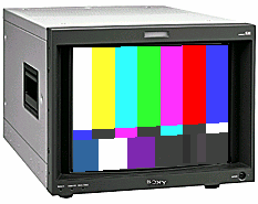
Symptom seen on monitor: 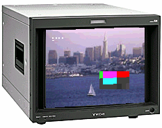
As can be seen, two possible defects are shown. One is a series of white "pinholes" in the upper left quadrant, and the other is a "block" of missing forground information, allowing the BG to peek through.
Switcher Test Setup
Set the switcher to display the fault clearly, using as little of an effect as possible. Once you have found the settings which exhibit the fault, you can proceed. Select input sources and an effect which make the fault clearly visible. Monochrome signals often work well if the fault is in the luminance channel, while red or blue fields work well if the fault is in one of the component channels. The idea to follow in selection of input signals for troubleshooting is to select those signals which cause the error to contrast sharply with the signal. Two signals which contrast sharply and are very simple, such as a black field applied to one input and a white field applied to another, achieve such a result. The reason for this is that you will be looking at data instead of analog video. Diverse analog signals such as bars or multiburst can look deceptively similar when viewed one bit at a time, but it is easy to tell a black field from a white field because in that case most of the bits are either set to 0 or 1 respectively. In any case, a full field signal is the best way to find problems.
How to trace the signal through the switcher:
Here's where the digital scope comes in. Say the error on the monitor screen can be seen plainly. Use the waveform monitor to find out what line(s) the error is displaying on, for example, a memory defect causes a small "hole" in the foreground to appear 6 microseconds into line 36 of every even field. Using channel 1 of the digital scope, trigger on that line using output video as the trigger source, and vary the timebase until you see the artifact plainly on the scope display. This is where a digital storage scope is very handy. A regular analog scope can trigger on and display this image, but it will be so dim that it will be almost impossible to see. Now that you have found a manifestation of the defect, leave channel 1 connected to that point, and use channel 2 to temporally compare the data at each testing point to the artifact.
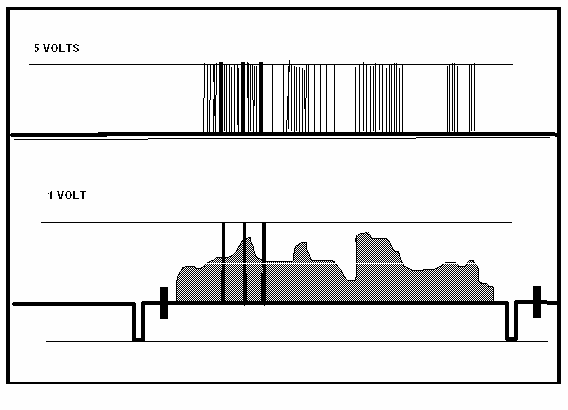
A sample digital scope screen is shown. Note the three signal spikes which remain fixed. These may represent stuck memory address bits which are being read out of memory into this line of video, and would correspond to the white "pinholes" of the above screen shots. The bit displayed on the scope screen is the MSB, only one of the 8 parallel bits used for each component. Any time the video signal must rise to more than 50%, the MSB is 1 rather than 0. Note the logic signal on the top trace is 5 volts and the video signal on the lower trace is 1 volt. Video DATA as shown above could be found almost anywhere in the DFS500, especially on the MY board. It is very likely that this kind of problem would be present in only one field.
If the defect occurs no matter what input is used:
Since the signals going into the switcher are good, and the signal coming out now clearly displays the fault, as well as the digital scope clearly displaying the fault, you can work 'backwards' towards the inputs. Going backwards from the output, you will trace the signal back through the line amplifiers, from the encoder. Let's say that you found the anomaly to exist on the luminance channel, but not on the component channels. Trace the signal back to the DAC. The DAC will have an 8 bit data bus input for each component, labeled x0 to x7. The digital signal stream flows through these parallel lines throughout the whole signal path (The signal path was selected when you adjusted the state of the switcher to display the anomaly). Checking each one of these, you will find that the anomaly occurs on one or more of them. It doesn't matter which one it occurs on, since you can use any instance of the anomaly to trace the digital signal back through the M/E towards the memory. Referring to the schematic, you will see that the data line you are checking goes to several multiplexer IC's. These IC's are not as complex as may seem at first glance, but the large number of pins can be intimidating. Multiplexers have several inputs and outputs composed of parallel data ports. One set of I/O ports is used for the for the video datastream at any one time, and another set of inputs is used to control the path of the stream inside the IC, selecting which input ports connect to which output ports, and even selecting which individual bits 0-7 of a particular input port are routed to a particular output port..
Switching Data vs. Video Data
At this point it should be mentioned that an anomaly may be caused by either corrupt video data or corrupt switching data. Switching data is temporally related to the effect transition, while video data is related to the instantaneous amplitude of the video signal.
Bad switching data, such as a repetitive bit error, often will cause a "pinhole" effect, letting the undistorted background show through a tiny area of the foreground on the video monitor. The pinhole can be more or less transparent, depending on which bit is affected. The MSB will have the most effect, while the LSB will produce a very much more occluded pinhole.
Bad video data of the same bitwise dimension often shows up as a pinhole of a fixed, incorrect, or noisy color, again, the intensity depending upon which bit is incorrect. Also note that the defect in either case can be any shape or size, not necessarily a "pinhole"-sized defect. Rectangular shapes are, however, very common.
An input signal that "bounces", that is, goes from full-field to zero every second can be useful in determining whether the defect is in the video data path or the switching data path. The bounce will show up on the good bits in the video data path, but will not show up in any bits in the switching data path, except for keying data paths, and then only if the Key is ON. If you have the effect set to "wipe", and move the fader, the effect transition will be visible in the switching data path, but only if your test point is after the IC that handles the transition.
For every DSP IC which is attached to a bus on which you find the bad data, check the same-numbered input bits on that IC to determine if the bad signal is passing through the IC. A set of colored pencils is useful to mark the lines in the complicated multi-page schematic. Once you find the bad bit at an input of a particular IC, refer again to the schematic to determine the sources from which that signal may come. This will lead you to yet more IC's. There may be 4, 5, or many more IC's between you and the point of failure. Repeat the procedure until you find a point in the circuitry where the defect is coming out of an IC, but apparently not going in. This may or may not be the bad IC. Carefully analyze the schematic and signals around this IC, to see if it is doing something interesting such as converting serial data to parallel, or if it is gating the data in some other way.
An example of this would be one of a pair of latches that switch the inputs of a matrix IC to the outputs from the field memories, where one is on during even fields and the other is on during odd fields. A fault in this kind of circuitry would be a switching data fault. If the data present in such circuitry agrees with the data controlling it, then the fault may be in a CPU, perhaps on the PU board. Understanding the function of each IC which is being checked is very helpful. Use the Manual or the Sony IC data books in the Library to find out about the IC's.
If the defect occurs on only one input:
Each currently selected input to a switcher has its own ADC and memory. If the input signal is composite, it is sent through a decoder to obtain the component signals, and each component is then passed to an ADC and converted to a parallel digital signal. The signal is then written to memory referenced to itself.
Read output from the memory is synchronized to reference. Alternate fields are sent to alternate blocks of memory. An input signal that "bounces", that is, goes from full-field to zero every second can be useful in determining which bit or bits are defective.
Reference the switcher and the scope to the input signal going to the offending input. Set the scope for triggering at the defect. You may have to adjust the scope for a delay or move the line trigger back and forth a few lines, depending on the switcher, in order to find the appropriate time window in which to look for the defect. Look at each bit from the ADC, and determine if one of the bits fails to make a state transition when the input signal is changed from black to white (again, assuming the luminance channel is under scrutiny).
A failure of this kind affects the entire time window of the video signal, and will cause an incorrect level of contrast. A posterization effect may be noticeable if the bad bit is one of the more significant. Trace the signal to the memory. Before it gets to the memory, it may pass through a latch or buffer. Check the outputs of each intervening device, all the way to the memory. If the data still looks good, you may assume that the switcher is at least trying to write the data to the memory. Check the outputs of the memory for the same data as was presented to the inputs. (This is where a bounce or flat-field signal is handy.) Note that the read data from the memory will be synchronized to the reference signal. Be sure to check the control signals for the memory as well. A missing field can be caused by a faulty control signal or a bad gate or latch.
Simple Fixes:
There aren't many, but the small soldered-in CP-Nxx fuses may cause odd symptoms. For example, an open PS1 on the MY-54 board will cause the loss of all effects except cut transitions. An open PS1 or PS2 on the DA-63 board can cause error 03 to display on the keyboard. The first thing to do when finding a problem that affects the entitre display is to check these fuses on each board. The fuses can intermittently have high resistances of 200-600 ohms; not quite open, but this is enough to cause low voltage for the memory and the resulting unusual images.
Also, please observe the position of the Control Select switch on the SY-72. It should be placed in the BVE900 position for most troubleshooting. Other positions cause the DFS to expect to be part of a system, and it will not function properly for standalone testing.
Questions