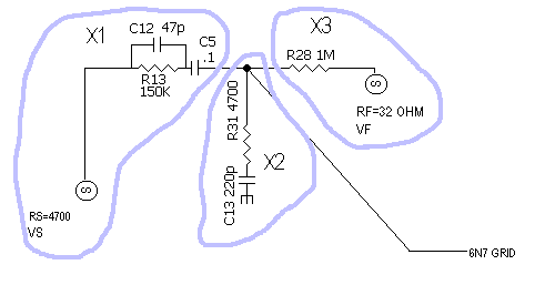
RS refers to the impedance of the drive source signal provided by the plate circuit of the 6SN7 and its 4700 ohm load resistor.
VS refers to the voltage present at that plate.
RF refers to the impedance of the feedback winding of the output transformer, which is 32 ohms in this case.
VS refers to the voltage provided by the feedback source (output transformer winding).
X1 refers to the impedance of the section circled with the "X1". X2 and X3 refer to the other sections respectively.
It can be seen that capacitive reactances aside, the network adds a certain amount of voltage from each source to create the composite signal voltage present at the 6N7 grid terminal. VF, the feedback signal, is supplied out of phase with VS, thereby detracting from the 6N7 grid drive and reducing the gain of the amplifier when, for a given input amplitude, the output signal is larger than desired.
The varying gain of the amplifier is not so much realized across the realm of input voltage level variation, but rather it is very evident in the frequency domain. The amplifier is designed with excess gain, perhaps 6-10 db. The feedback network smooths out the frequency response using the excess gain at various 'troublesome' frequencies (usually extremes of the output transformer's designed audio spectrum: lack of iron at low frequencies and excessive phase shift at high frequencies).
The following table shows calculated impedances at 10Hz, 1KHz, and 30KHz. The estimated gains shows do not include deviations caused by frequency-dependent deviations in the output stage; i.e., we assume a perfectly balanced set of tubes and ignore the frequency domain effects of any coupling capacitors and cathode resistor bypass capacitors not included in the network under examination.
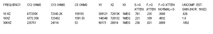
Calculations were made for the reactances of the capacitors in the network, as well as the impedances of each part X1 through X3 of the network. Impedances are in Ohms, K=1000, M=1000000.
The "S->G ATTEN" column shows the ratio of delivered grid voltage divided by the voltage present at the 6SN7 plate which is the terminal VS on the network schematic.
The "F->G ATTEN" column shows the ratio of delivered grid voltage divided by the voltage present at the output transformer feedback winding which is the terminal VF on the network schematic.
The column "F->G ATTEN NORMAL<-S" shows the ratio of feedback voltage attenuation divided by the source voltage attenuation.
The column "UNCOMP. EST. GAIN (NOR. 1KHZ)" shows the relative gain of the amplifier if it were perfectly corrected by the network at each of the three frequencies. This can be thought of as the small signal open loop frequency response.
Please keep in mind that these are very rough approximations, and do not (I reiterate) include the effects of coupling capacitors nor of cathode bias resistor bypass capacitors.
The terms have been dealt with in a manner to greatly simplify the explanation. If any mistakes are found in the document, or if you find it useful, please advise.